The ranking of intelligent driving chips is not simply based on AI computing power. CPU, storage bandwidth, power consumption, and AI computing power values are equally important.
In intelligent driving systems, CPU computing power plays a crucial role. Due to the complexity of software systems, they require a significant amount of CPU computing resources. The software system includes numerous middleware such as SOME/IP, adaptive AUTOSAR, DDS, ROS, etc., as well as basic software such as customized Linux BSP, OS abstraction layer, virtual machine, etc. In addition, memory management, various drivers, communication protocols, etc. associated with underlying hardware also consume a significant amount of CPU resources
In the application layer, path planning, high-precision mapping, and behavioral decision-making are also the main consumption parts of CPU resources. At the same time, the CPU is also responsible for managing tasks such as task scheduling and storing and handling instructions during AI operations. Although AI plays an important role in image feature extraction, classification, BEV transformation, vector map mapping, or spatial distribution, the CPU remains the core, while AI is only its subsidiary function.
In terms of measuring computing power, the weighted rankings are AI computing power, storage bandwidth, CPU computing power, GPU computing power, and manufacturing process. Storage bandwidth and AI computing power are equally important. Although GPUs can process FP32 data in some cases and play an important role, most in car AI processing parts only correspond to INT8 bit data.
In order to measure computing power more accurately, the number of MAC arrays is a key indicator. For example, Google's TPU V1 has 65000 FP16 MAC, operates at a frequency of 0.7GHz, and has a computing power of 91TOPS. The two NPUs of Tesla's first generation FSD, each with 9216 INT8 MAC, operate at a frequency of 2GHz, and have a total computing power of 73.7TOPS. As for manufacturing processes, more advanced processes mean lower power consumption
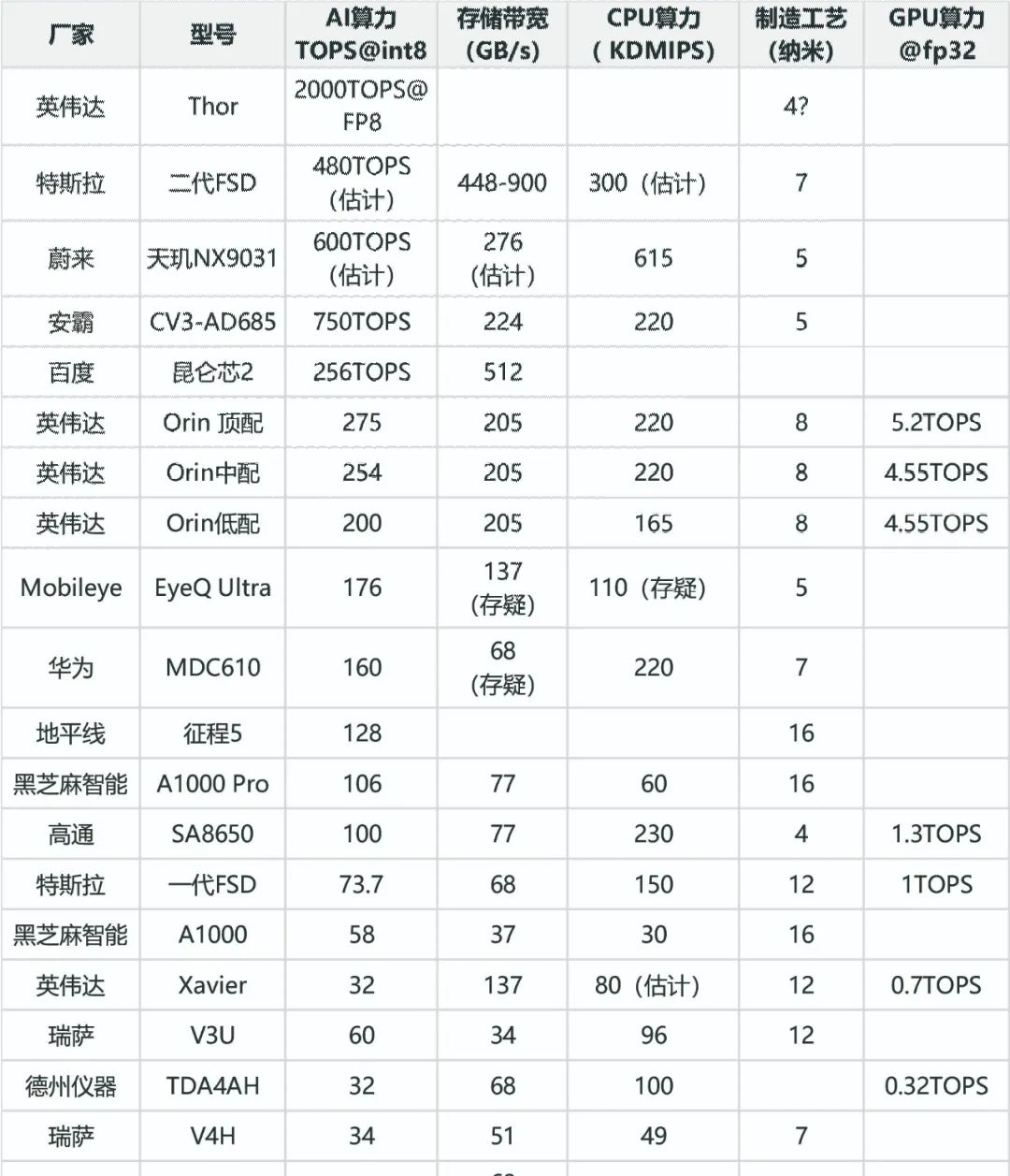
Top 20 intelligent driving chips
How to calculate storage bandwidth? The chip itself has a storage manager, which is usually a part of the CPU. There are two factors that determine storage bandwidth: first, the type of storage supported by the CPU, namely the physical layer and controller of the storage, and second, the storage bandwidth of the CPU. The storage bandwidth of LPDDR is generally up to 256 bits, GDDR can reach 384 bits, and HBM can reach 4096 or even 8192 bits, all of which are related to costs. When designing the chip, manufacturers, We will find a balance between cost and performance. Some manufacturers prioritize cost, with 64 bits or even 32 bits, while others prioritize performance. For example, true AI chips are all HBM chips, with costs exceeding $1500.
Comparison of Common Automotive Memory Performance and Price
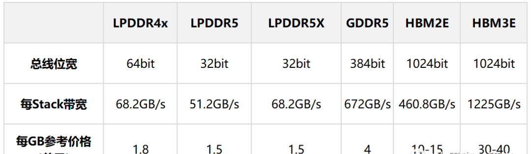
The above table shows the performance and price comparison of common car memory. Obviously, you get what you pay for. Nvidia H100 is the largest purchaser of HBM3, with a purchase price of approximately $14 per GB. Another point to point out is that there is currently no automotive grade GDDR6 storage chip available.
At present, except for Baidu and Tesla, all intelligent driving chips use LPDDR.
The parameters of LPDDR throughout history
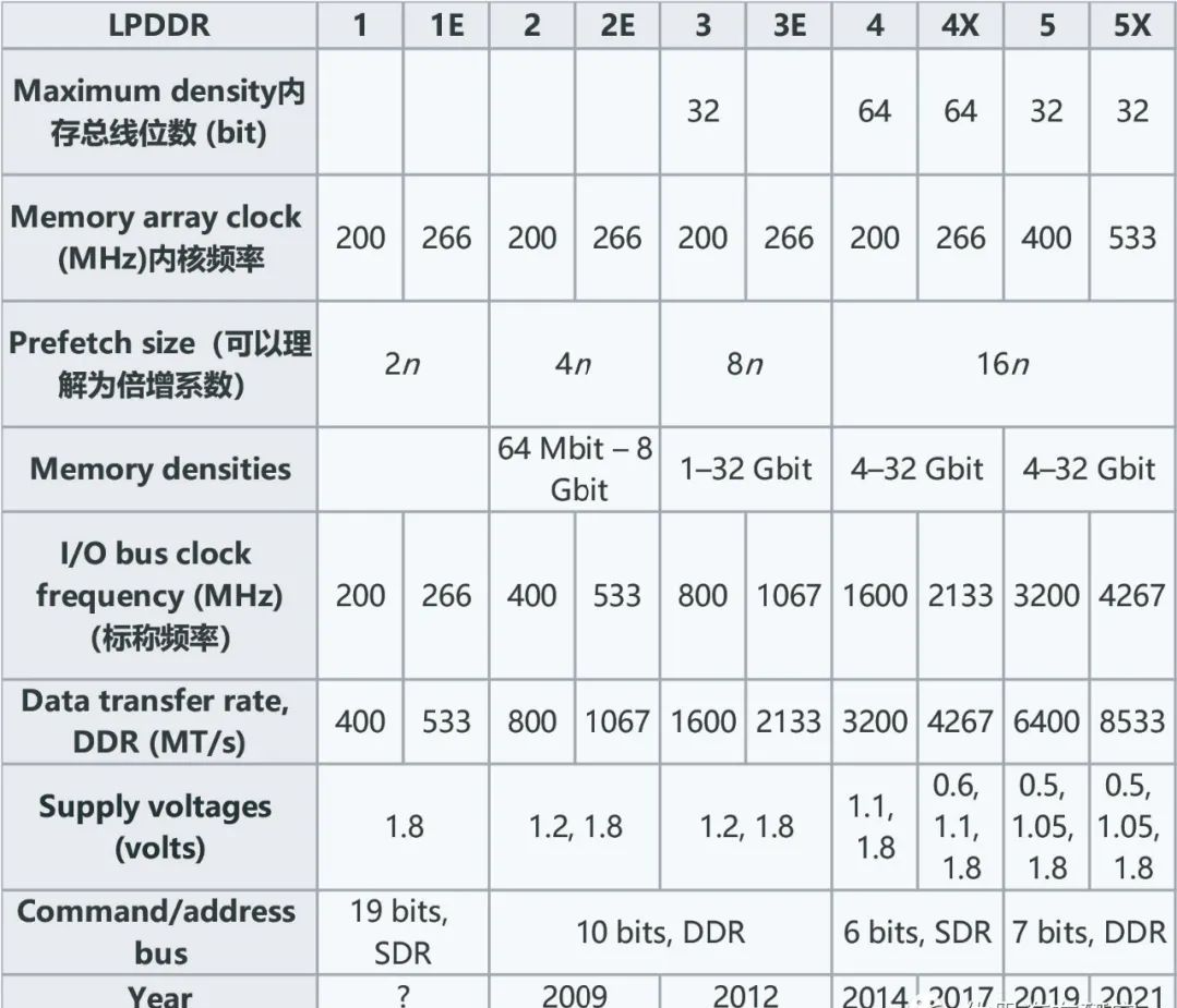
Storage bandwidth plays a crucial role in intelligent driving systems, calculated by multiplying the CPU's storage bit width with the Data Transfer Rate (DDR) of the memory, and then dividing it by 8 to convert it to uppercase GB. Taking NVIDIA Orin and Tesla's first generation FSD as examples, Orin has a storage bit width of 256 bits, supports LPDDR5, a transmission rate of 6400MT/s, and a storage bandwidth of 204.8GB/s; Tesla's first generation FSD has a storage bit width of 128 bits, supports LPDDR4, a transmission rate of 3200MT/s, and a storage bandwidth of 51.2GB/s.
The Roof line model is a theoretical tool for solving computational and visitor stock problems. The computational complexity refers to the number of floating-point operations that occur in a complete forward propagation of a model, which is the time complexity of the model. The visiting stock refers to the total amount of memory exchange that occurs during a forward propagation process of the model, which is the spatial complexity of the model. The computational power I of the model can be obtained by dividing the computational power by the number of visits, indicating how many floating-point operations the model uses per Byte of memory swapping during the calculation process.
Due to the exceptionally complex nature of the intelligent driving system software, it consumes a large amount of CPU computing resources. The software system includes numerous middleware such as SOME/IP, adaptive AUTOSAR, DDS, ROS, etc. The basic software includes customized Linux BSP, OS abstraction layer, virtual machine, etc. In addition, path planning, high-precision mapping, and behavioral decision-making in the application layer also consume a large amount of CPU resources. At the same time, the CPU also manages task scheduling, storage and handling instructions during AI operations, and overall task scheduling and decision-making are naturally the tasks of the CPU.
In intelligent driving systems, CPU computing power occupies a core position. In order to ensure the smooth operation and efficient performance of the system, multiple factors such as AI computing power, storage bandwidth, CPU and GPU computing power, and manufacturing process must be comprehensively considered.
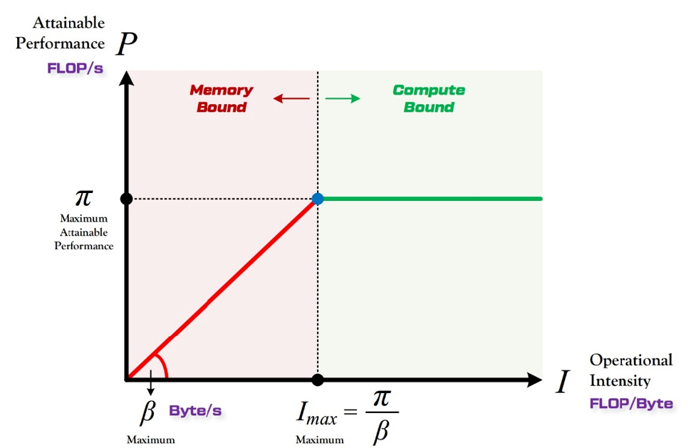
Computing power determines the height of the roof (green line segment), while bandwidth determines the slope of the eaves (red line segment)
In intelligent driving systems, the theoretical performance of model calculations is limited by the maximum theoretical performance of hardware. If the required computing power of a model exceeds the theoretical performance of the computing platform, the utilization rate of the computing platform will reach 100%. At this time, the risk is that the frame rate of the processed image or FPS may not reach the target frame rate. For intelligent driving, the mainstream frame rate is 30FPS, while high-speed driving requires a higher frame rate.
If the computational power requirement of the model is too high, the computing platform cannot adapt even when running at full load, resulting in a decrease in frame rate. In this situation, driving at high speeds can bring risks. Generally speaking, manufacturers do not recommend using models that require computing power far beyond the theoretical performance limit.
When the utilization rate of the computing platform is below 100%, the model is in a Memory Bond state. In this state, the theoretical performance P of the model is entirely determined by the upper bandwidth limit of the computing platform (slope of the eaves) and the computational intensity I (Intensity) of the model itself. Therefore, under the premise of bandwidth bottleneck, the steeper the bandwidth of the computing platform or the greater the computational intensity of the model, the theoretical performance P of the model can grow linearly.
A lower slope means that even if the computational intensity increases rapidly, the increase in computing power of the computing platform is slow, resulting in a low utilization rate of the computing platform. For example, if the theoretical computing power of a computing platform is 100TOPS and the slope is very low, even a high computational intensity model may have a utilization rate of less than 50%. This means that storage bandwidth determines the performance utilization of the computing platform. Therefore, the importance of storage bandwidth is no less important than computing power, and may even be higher than computing power. This is also the main reason why Tesla's second-generation FSD ranks second, as GDDR6 has an overwhelming bandwidth advantage over LPDDR.
Tesla's second-generation FSD
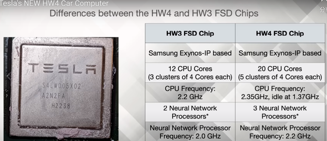
Tesla's second-generation FSD chip adopts Samsung's 7-nanometer process, which is mainly due to price and geographical considerations. Firstly, Samsung's contract manufacturing price is much lower than TSMC's, only about half of TSMC's price. Secondly, TSMC's Arizona factory has relatively low efficiency, with slow progress from construction starting in 2020 to expected production in 2025. Samsung's Dexas Austin second-generation factory was completed and put into operation in just two years, and it is relatively close to Tesla headquarters.
The first generation FSD used Samsung's 14 nanometer process. According to WikiChip data, the transistor density of Samsung's 7-nanometer LPP HD high-density cell scheme is as high as 95.08 MTr/mm ², The transistor density of HP's high-performance solution is 77.01 MTr/mm ²。 In contrast, the transistor density of Samsung's 14nm UHP scheme is 26.22 MTr/mm ², The HP scheme transistor density is 32.94 MTr/mm ²。 Basically, Samsung's transistor density of 7 nanometers is more than three times that of 14 nanometers. This means that Tesla's second-generation FSD chips can accommodate more MAC arrays, achieving a triple improvement in AI performance. Considering the AI performance of the first generation FSD 73.7TOPS@INT8 A triple increase is 221.1TOPS. If combined with sparse model acceleration technology, the number of computing power can be doubled. Furthermore, it is speculated that due to the significantly larger area of the second-generation FSD chip compared to the first generation, and the increase in NPUs to three, its computing power may be around 500TOPS.
Tesla has also significantly enhanced CPU performance in the second-generation FSD, adopting Samsung's Exynos 20 core configuration. This further proves the importance of CPU in intelligent driving.
Anba's CV3 may not be well-known to most people, but it performs well in storage bandwidth, supports the highest LPDDR5X specification, and has the highest 256 bit width. This chip is manufactured using Samsung's 5-nanometer process and has currently received support from Continental Automotive in Germany.
In summary, both Tesla and Anbar are actively exploring more advanced process and storage technologies to improve AI performance and overall system performance. With the continuous development of intelligent driving technology, these innovations will bring more efficient and safer driving experiences to future cars.
Internal framework diagram of Anba CV3-AD
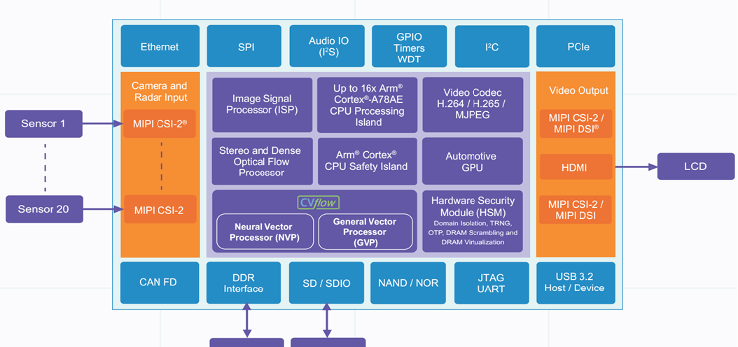
Anba CV3-AD is a high-performance automotive AI chip that includes up to 16 cores of the Coretex-A78AE, with extremely high CPU computing power. At the same time, it has also passed ASIL-B certification, which means it has high reliability and security. In terms of AI computing power, Anba CV3-AD is equivalent to 500TOPS and performs excellently.
Nvidia, Tesla, and Mobileye are also well-known companies in the field of automotive AI chips. Nvidia's chips have a bit width of 256 bits, while Tesla and Mobileye's chips mostly have a bit width of 128 bits. As for the storage information of Journey 6, it has not been disclosed yet.
Additionally, it is worth mentioning Kunlun Chip Technology, a subsidiary of Baidu. Although less well-known, Kunlun Chip Technology is actually a product of Baidu's independent Intelligent Chip and Architecture Department, officially known as Kunlun Chip (Beijing) Technology Co., Ltd. The company completed independent financing in April 2021, with a valuation of approximately 13 billion yuan. On November 29, 2022, during Baidu Apollo Day Technology Open Day, the second generation Kunlun chip announced that it had completed the complete adaptation on the driving system of Baidu's autonomous vehicle RoboTaxi and was running normally in the advanced autonomous driving system.
The history of Kunlun Chip Technology can be traced back to 2011, when it began working on AI computing and early used FPGA chips to accelerate AI computation. In the following years, Kunlun Chip Technology deployed over 5000 FPGA chips in Baidu's data center, and in 2017, it deployed over 12000 chips. In 2018, Kunlun Chip Technology decided to independently develop AI chips and officially launched the research and design of Kunlun Chip series products.
The first generation Kunlun chips began large-scale deployment in 2020, using 14 nanometer technology and advanced HBM memory and 2.5D packaging technology. This chip has been deployed in over 20000 Baidu data centers since its mass production. One year later, the second generation Kunlun chips were mass-produced using more advanced 7-nanometer technology and XPU second-generation architecture. Meanwhile, it is also the first AI chip in the industry to adopt GDDR6 high-speed memory technology. At present, Kunlun Xin Technology is developing more advanced third-generation AI chips, and may launch customized high-performance SoCs (system level chips) for advanced autonomous driving systems in the future.
In summary, the market competition in the field of automotive AI chips is fierce, and major manufacturers are actively developing high-performance, high reliability, and high safety products. With the continuous progress of technology and the expansion of application scenarios, there is still great development space and potential in this market.

Nvidia has always attached great importance to storage systems, with a maximum of 256 bits across the entire line. The Qualcomm SA8650 is very similar to the SA8255 in the cockpit field, with a CPU and GPU that are basically the same. The AI computing power has been specially enhanced, and the storage bit width is a relatively rare 96 bits. The SA8650 replaces the previous generation SA8540P, mainly by adding a section for functional safety and adding four Cortex-R52 cores. Mobileye attaches great importance to cost and never discloses its storage bandwidth and supported storage types, only guessing. Although Xavier is an early product, its storage bit width is the highest at 256 bits, so it ranks very high.


WeChat official account

Official Tiktok number
Fax: 0086-755-85274635
Address: Building 22, Hongrongyuan North Station Center, North Station Community, Minzhi Street, Longhua District, Shenzhen
© Copyright © 2023 Shenzhen Enchey Technology Co., Ltd 粤ICP备2023150117号